FIRST by FMD: Accelerating Europe’s semiconductor future with the APECS pilot line

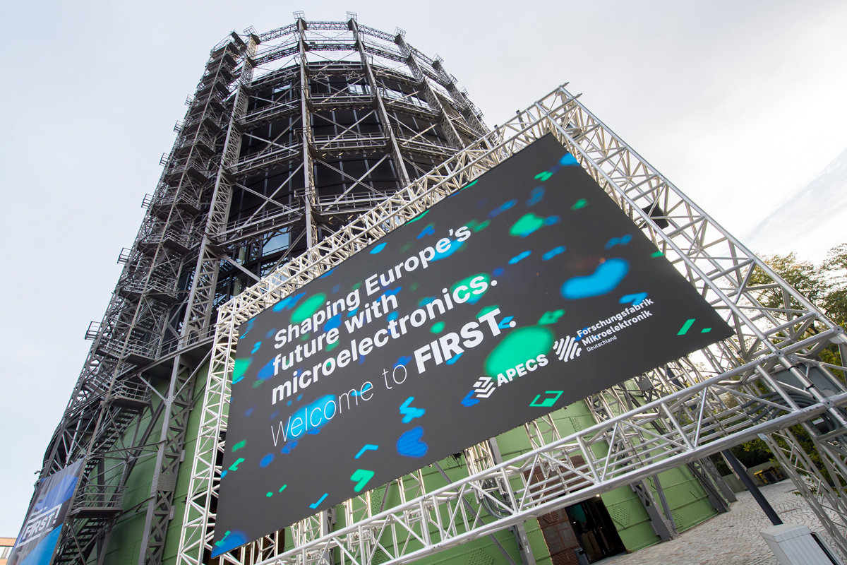
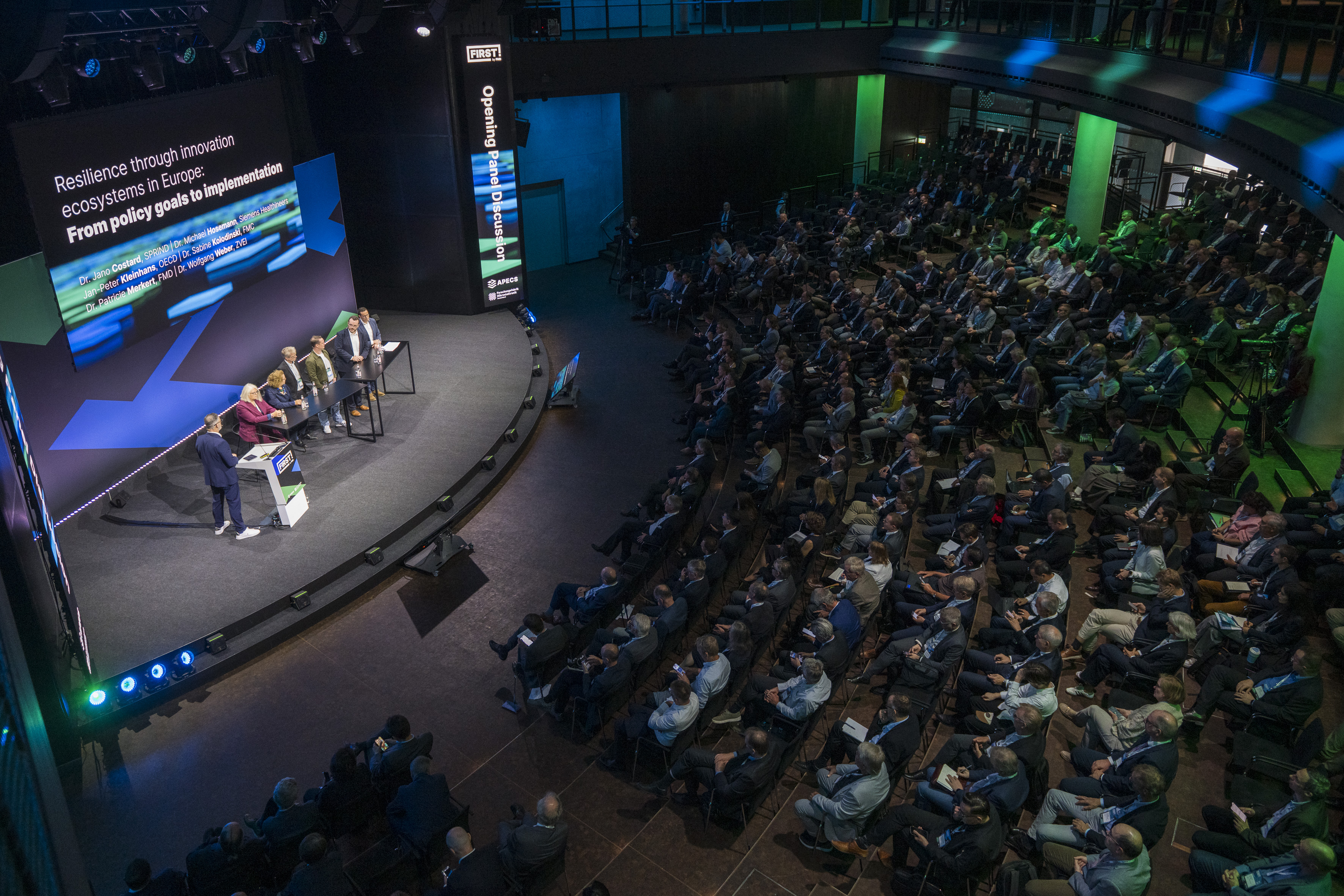
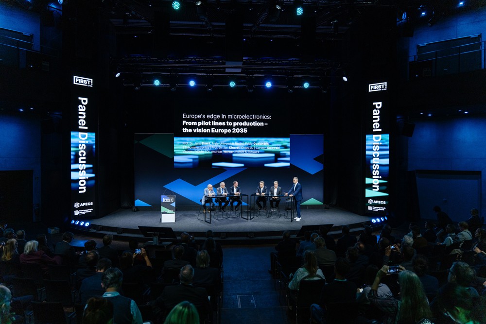
More than 500 industry leaders, researchers, and policymakers gathered in Berlin to discuss Europe’s semiconductor future, with the APECS pilot line taking center stage as a catalyst for faster technology transfer and European chiplet innovation.

Under the theme “Shaping Europe’s Future with Semiconductors,” FIRST by FMD brought together key players from across Europe’s microelectronics ecosystem to address one of the industry’s most pressing challenges: How can Europe translate its strong research capabilities into scalable technologies, competitive products, and greater technological resilience?

The two-day event, organized by the Research Fab Microelectronics Germany (FMD), focused on the conditions needed to strengthen Europe’s semiconductor ecosystem — from technology transfer and industrial infrastructure to advanced packaging, chiplets, design capabilities, and strategic collaboration across the value chain.

Recap Video

Clicking the button will play a YouTube video; youtube.com uses cookies.

Prof. Dr. Holger Hanselka (President of Fraunhofer-Gesellschaft)

© Fraunhofer Mikroelektronik
Prof. Dr. Holger Hanselka (r.)

»Europe’s future in microelectronics will not be determined solely by roadmaps and work in laboratories, but by the joint commitment of industry and academia to rapidly translate research excellence into scalable industrial technologies.«

From research excellence to industrial reality

© Fraunhofer Mikroelektronik

The central message throughout FIRST by FMD was clear: Europe does not lack semiconductor research excellence. The challenge is creating efficient pathways that allow promising technologies to move from the laboratory into industrial applications.

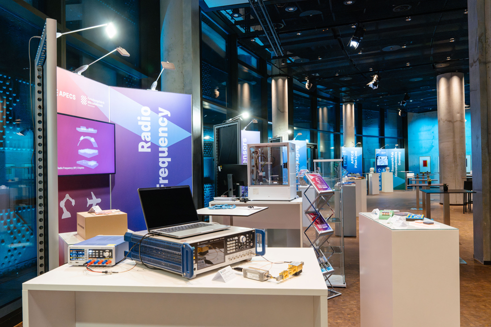
That requires more than technology roadmaps. Companies and research institutions need access to development environments, advanced equipment, validated processes, and infrastructure that allows technologies to be tested and further developed under realistic industrial conditions. This is where the APECS pilot line comes in.

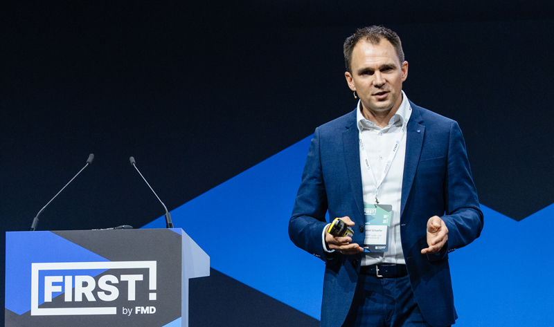
Marcel Schäfer (TRUMPF)

© Fraunhofer Mikroelektronik
Marcel Schäfer (TRUMPF)

»Advanced Packaging is the next battlefield. Europe needs packaging sovereignty alongside fab sovereignty. Laser beam-shaping enables chiplet integration at scale«

APECS takes center stage

© Fraunhofer Mikroelektronik

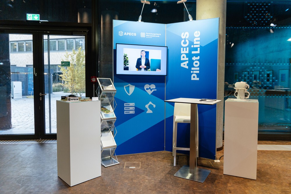
The importance of the APECS pilot line became particularly visible on the second day of FIRST by FMD, when the program shifted from strategic perspectives toward concrete technologies, applications, and industrial implementation.

The session “APECS pilot line – European chiplet innovation” highlighted how chiplet architectures and advanced packaging can contribute to Europe’s technological resilience. Rather than relying on increasingly complex monolithic chips, chiplet-based architectures enable different technologies and functions to be combined within a single system.

This approach creates new opportunities for system design — but it also introduces new challenges in integration, packaging, testing, and manufacturing. The APECS pilot line is intended to address exactly these challenges by providing a European environment in which companies and research institutions can develop and validate new approaches under realistic conditions.

From chiplets to market readiness

A second session dedicated specifically to the APECS pilot line and European chiplet innovation brought together perspectives from across the semiconductor value chain.

Dr. Klaus Beilenhoff of United Monolithic Semiconductors, Dr. Eric Fribourg-Blanc of the Chips Joint Undertaking, Matthias Gläßer of JENOPTIK Optical Systems, Nikolaus Hahne of Quantune Technologies, Lars Lust of Swissbit, and Dr. Dirk Schumann of FMD discussed how advanced packaging and heterogeneous integration can open new possibilities for chiplet-based systems.

The discussion went beyond technology itself. A key question was how these technologies can become accessible to companies today, and how Europe can move from promising concepts to market-ready solutions. That means addressing practical questions around process development, technology validation, access to infrastructure, industrial requirements, and scalability.

In this context, the APECS pilot line is more than a technology platform. It is an innovation infrastructure designed to shorten the path from idea to industrial application.

The broader FIRST by FMD program reinforced why this capability is becoming increasingly important.

Dr. Dirk Schumann (FMD)

© Fraunhofer Mikroelektronik
Dr. Dirk Schumann (Research Fab Microelectronics Germany, FMD)


»FMD connects the required capabilities through one reliable partner across the innovation journey. Industrial R&D remains in the lead. But companies no longer have to build and manage the entire technology chain on their own. The result is clear: fewer interfaces, faster decisions and a shorter path from feasibility to an industrially usable solution.«

Advanced packaging as a strategic capability

© Fraunhofer Mikroelektronik
Rolf Aschenbrenner (Fraunhofer IZM)
© Fraunhofer Mikroelektronik
Manuela Junghähnel (Fraunhofer IZM)
© Fraunhofer Mikroelektronik
Dr. Erin Lavigne (NY Creates)

In “Microelectronics for Tomorrow,” Rolf Aschenbrenner of Fraunhofer IZM/FMD and Hannes Voraberger of AT&S examined the new integration, performance, and system architecture requirements emerging from AI and quantum technologies.

The discussion highlighted a fundamental shift in semiconductor development: performance is no longer determined by the individual chip alone. Increasingly, the way different components are integrated into a system becomes a critical source of innovation.

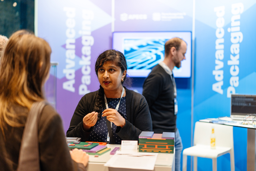
This perspective was taken further in the session “Advanced Packaging in the AI Era.” Harald Gossner of Intel, Dr. Manuela Junghähnel of Fraunhofer IZM-ASSID/FMD, Dr. Erin Lavigne of NY Creates, and Henk Niesing of ASML discussed heterogeneous integration and 2.5D and 3D approaches, and their growing importance for product development, time-to-market, and industrial value creation.

For Europe, this underlines the strategic relevance of initiatives such as APECS: advanced packaging is no longer simply a back-end manufacturing topic. It is becoming a core element of system innovation and semiconductor competitiveness.

Building a European chiplet ecosystem

FIRST by FMD also demonstrated that the success of advanced packaging and chiplet technologies will depend on collaboration across traditional industry boundaries.

Design houses, semiconductor manufacturers, packaging specialists, equipment suppliers, research organizations, startups, and established industrial players all contribute different capabilities to the emerging ecosystem. The APECS pilot line can provide a common environment in which these capabilities come together.

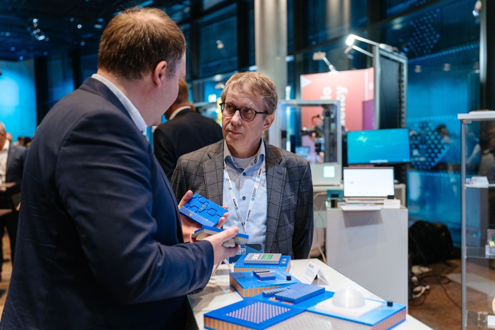
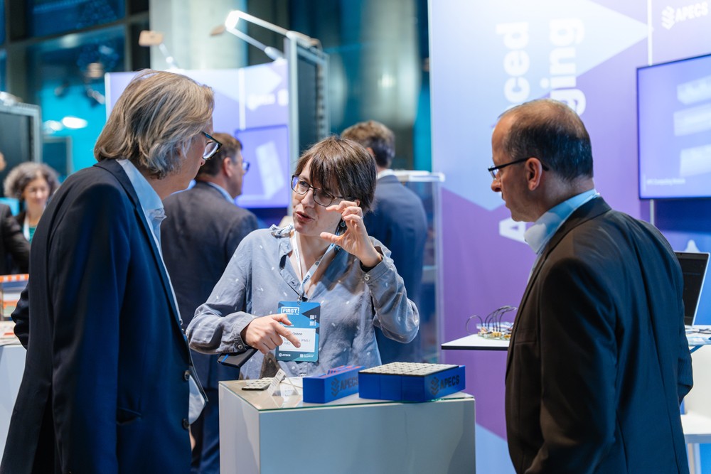
This collaborative approach is particularly important for smaller companies and research teams that may not have access to the infrastructure required to develop and validate advanced integration technologies on their own.

By lowering barriers to access and enabling industry-oriented development, APECS can help turn European research and engineering capabilities into technologies that are ready for industrial adoption.

© Fraunhofer Mikroelektronik
Final panel »Beyond technology: Talent, skills, and sustainable workforce models for semiconductor excellence«
© Fraunhofer Mikroelektronik

Beyond technology: building the workforce to match

The final panel, “Beyond Technology: Talent, Skills, and Sustainable Workforce Models for Semiconductor Excellence,” brought the discussion back to one of the most fundamental requirements for Europe’s semiconductor ambitions: people.

Frank Bösenberg of Silicon Saxony, Katharina Kunze of Microtec Academy, Prof. Dr. Thomas Mikolajick of TU Dresden/ForLab, and Prof. Dr. Norbert Wehn of RPTU Kaiserslautern-Landau/Chipdesign Germany discussed the specialized skills and sustainable workforce models required to support a high-performing semiconductor industry.

The message complemented the discussions around APECS: infrastructure can accelerate innovation, but skilled people are needed to operate it, develop new technologies, and turn them into products.

A practical step toward Europe’s semiconductor future

The first edition of FIRST by FMD showed that Europe’s semiconductor strategy is increasingly moving from ambition to implementation. The discussions around the APECS pilot line illustrated what this implementation can look like in practice: creating accessible, industry-oriented infrastructure; connecting research with companies; enabling the development and validation of advanced packaging and chiplet technologies; and building pathways toward scalable production.

As semiconductor architectures become more heterogeneous and system integration becomes increasingly important, the ability to develop, test, and industrialize these technologies will be a critical competitive factor.

APECS is designed to provide that bridge.

And FIRST by FMD provided a forum for the European semiconductor community to discuss how that bridge can be used, and how collaboration across research, industry, and policy can help Europe turn technological excellence into industrial strength.

The overarching takeaway from Berlin was therefore not simply that Europe needs more semiconductor innovation. Europe needs faster, more connected pathways from innovation to industrial impact. The APECS pilot line is one important piece of that puzzle.

Upcoming Events

Chips JU Workshop

FMD's workshop recommendation: "Workshop on System-level design for the work programme 2027 of the Chips JU"


APECS Events & Roadshows

Get an overview of APECS-related events and roadshows all over Europe where our experts will be present.