About us

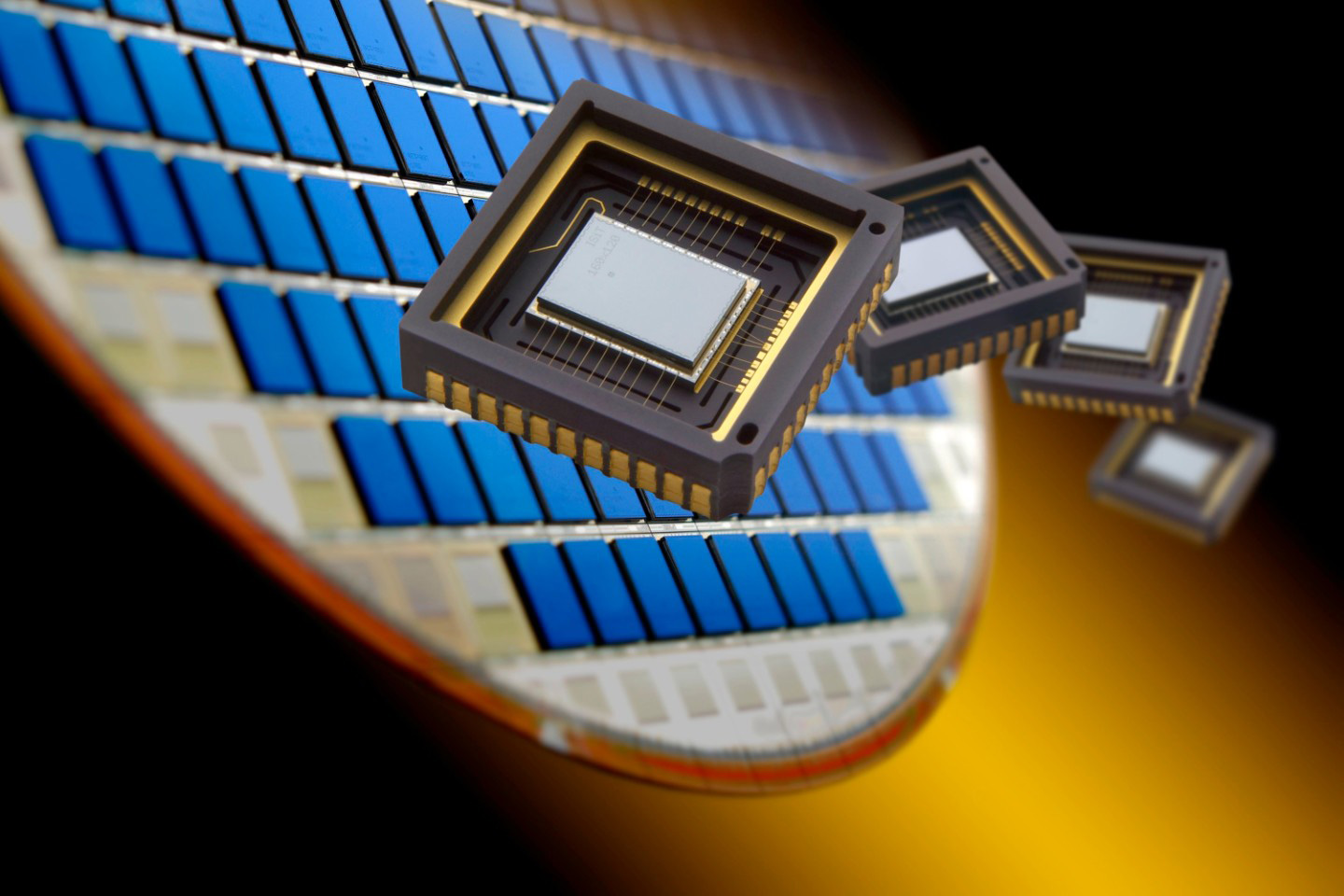
Pilot Line for Advanced Packaging and Heterogeneous Integration for Electronic Components and Systems (APECS)

As part of the EU Chips Act the APECS pilot line marks a major leap forward in strengthening Europe’s semiconductor manufacturing capabilities and chiplet innovation. By providing large industry players, SMEs, and start-ups with easier access to cutting-edge technology, the APECS pilot line will build a strong foundation for resilient and robust European semiconductor supply chains.

Within APECS, the institutes collaborating within the Research Fab Microelectronics Germany (FMD) are working closely with other European partners, making a significant contribution to the European Union´s goals of increasing technological resilience, strengthening cross-border collaboration and enhancing its global competitiveness in the semiconductor technologies.

Find out more about FMD's previous work and publications on the subject of chiplet technologies, system integration and system design on the FMD website.


APECS is the novel pan-European pilot line to establish a groundbreaking infrastructure for heterogeneous integration and advanced packaging:

By combining the know-how of ten European partners APECS will offer services, capabilities and training for European companies and research organizations to integrate and package chiplets and further advanced electronic components into novel electronic systems.

By joining forces of Europes´ leading RTOs, the platform of capabilities to be developed will include novel characterization, quality assurance, testing & reliability methodologies and a System-Technology Co-Optimization (STCO) design framework to ensure quality, reliability, security, green manufacturing and fast production ramp-up in collaboration with manufacturing organizations.

APECS focuses on bridging application-oriented research with innovative developments in heterogeneous integration, in particular emerging chiplet technologies. By pushing beyond conventional system-in-package (SiP) methods, APECS will deliver robust and trusted heterogeneous systems, significantly boosting the innovation capacity of the European semiconductor industry.


chiplet close-up
© Fraunhofer IZM
scientist in lab
© FBH
chiplet close-up
© Fraunhofer ISIT

Europe's investment in semiconductor research, through strategic projects such as APECS in the EU Chips Act, is crucial to reduce our dependence on international supply chains that are heavily concentrated in other regions. By boosting technological sovereignty, we are securing Europe's long-term economic stability and positioning the EU as an indispensable partner in the technological breakthroughs that lie ahead for the digital age. Furthermore, APECS will play a pivotal role in Europe's transition towards a carbon-neutral and circular economy through its promotion on eco-design and green manufacturing initiatives.

APECS will be a key driver of collaboration among European RTOs, industry and academia, fostering a lively innovation ecosystem. Customers will benefit from a single point of contact to the APECS pilot line. APECS covers end-to-end design and pilot production capabilities, to accelerate progress from cutting-edge research to practical, scalable manufacturing solutions.

The APECS consortium brings together the technological competences, infrastructure, and know-how of ten partners from eight European countries: Germany (Fraunhofer-Gesellschaft as coordinator, FBH, IHP), France (CEA-Leti), Belgium (imec), Finland (VTT), Austria (TU Graz), Greece (FORTH), Spain (IMB-CNM, CSIC) and Portugal (INL).

Expected outcomes of APECS

Advanced technologies for customized applications:
APECS provides Europe with innovation capabilities in advanced packaging and heterogeneous system integration based on chiplets, QMI, RF, opto, sensor and passive components, demonstrating the versatility and customizability of our technologies, but also responding to the emerging needs across different industrial sectors.​

A strengthened ecosystem:
APECS should bolster the European supply chain for semiconductor manufacturing by creating links between RTOs, manufacturers, material and equipment suppliers, design houses, Startups, SMEs and foundries. ​

Accessibility over the long run:
A long-term sustainable pilot line that grants SMEs and Startups long-term autonomous access to the services, portfolio, and infrastructure set up for them.​

Reduced Time-to-Market:
APECS aims to complete the design of innovative processes for advanced heterogeneous integration, spanning from the initial design phase through characterization to testing. This comprehensive approach will ensure a holistic development path, easing the transfer of ideas from conception to realization.​

Smooth knowledge transfer:​
The APECS pilot line eases smooth and reliable knowledge transfer between RTOs to speed up made-in-Europe innovation.​

Characterization, Test & Reliability (Test CTR):​
In which new concepts for quality assurance, safety and yield improvement are developed and made available.​

Demonstrators:
To validate the achievements of the developed design and technologies covering the different domains of application.​

The holistic system design ​(P/ADK design flows)​:
As access to an efficient and robust design environment for fully integrated systems as well as the basic ability to create system designs in the new technologies.​

Attracting and retaining talent:
The APECS pilot line places the microelectronics sector’s appeal at the center of the public agenda to drive new talent into the sector and tackle the shortage of skilled workforce.​


FAQ


Everything you need to know about the APECS pilot line.


Funding

APECS is co-funded by the Chips Joint Undertaking and national funding authorities of Austria, Belgium, Finland, France, Germany, Greece, Portugal, Spain, through the Chips for Europe Initiative.

Thanks to substantial funding from the German Federal Ministry of Research, Technology and Space (BMFTR)  and the federal states of Saxony, Berlin, Bavaria, Schleswig-Holstein, Baden-Württemberg, North Rhine-Westphalia, Brandenburg, and Saxony-Anhalt, it will be possible to further expand the R&D infrastructure in the coming years within the framework of the APECS pilot line.

Chips JU & EU logo
Logos of project sponsors