Access for start-ups

APECS is actively lowering the threshold for access to heterogenous integration for SMEs and start-ups. Here’s what we offer:
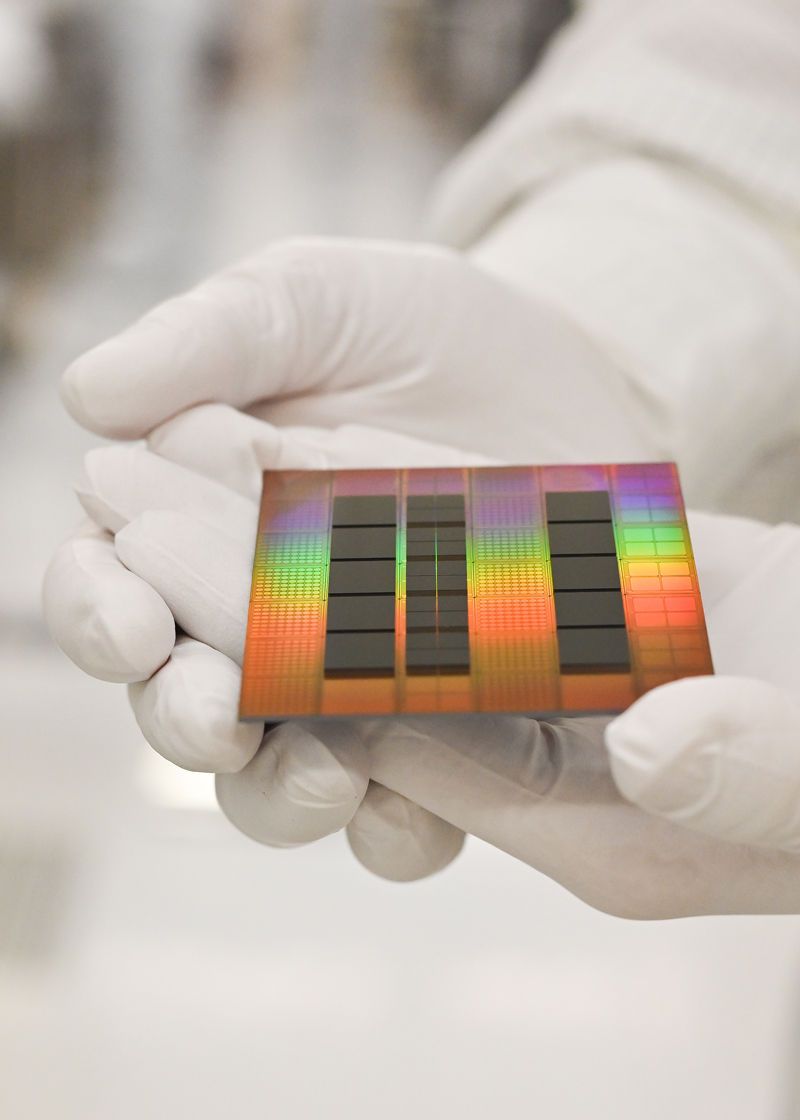
© Fraunhofer IZM-ASSID
Chiplet integration with die-to-wafer hybrid bonding.
  • Access to special technology: APECS will provide open access in accordance with the Chips Act requirements by providing support to integrated production facilities and open EU foundries, SMEs and start-ups, through preferential access to our pilot line. The fair access terms consider inclusivity of a diverse range of users across the EU, transparency regarding the selection criteria, processes, and terms governing access to the pilot line and non-discrimination to avoid potentially biased treatment of potential users based on their geographic location, affiliation, etc.
  • Prospect to create technology start-up without own cleanroom: APECS organizes the implementation process and helps optimize project execution. SMEs and start-ups that require additional support to accelerate the development of their proof-of-concept proposals are guided to the most suitable process lines and development units by our team. Bbased on the information and support provided, users choose the most suitable pathway for the integration of heterogeneous systems that best meets their specific requirements.
  • Growth through collaboration: Chiplet technologies require collaboration among semiconductor companies, design firms, equipment and material suppliers, and manufacturing partners to develop standardized interfaces and design methodologies. This collaboration fosters ecosystem growth and enables smaller companies to participate in the development of advanced semiconductor solutions and create new business opportunities for both established companies and start-ups.

APEC's service include:

  • Design and realization of innovative chiplet and chiplet-based systems tailored to specific customer applications, covering the entire spectrum from design till to characterization: This covers the whole design till characterization process based on customer specifications.
  • Creation of chiplet-related intellectual property (IP) generated from customer specifications: This not only adds value to the customer's technological portfolio but also enhances their competitive edge in the rapidly evolving microelectronics landscape.
  • Execution of tests for new chiplet process concepts within customer-specific fabrication processes: Such testing validates the feasibility and efficiency of these concepts, paving the way for their seamless integration into commercial production lines from for Lab-to-Fab.
  • Conducting machine and material testing utilizing the extensive fabrication machinery available within the pilot line: This enables a detailed assessment of materials and machinery equipment under various conditions, ensuring optimal performance and reliability in manufacturing processes.
  • Implementing advanced heterogeneous integration techniques on customer-specified materials: This service leverages the cutting-edge capabilities of APECS to offer tailored solutions that meet the evolving demands of the microelectronics, MEMS, and optoelectronics market segment.

APECS allows flexible entry- and exit-points for start-ups, offering singular innovations or the full flow of the workstream for advanced heterogeneous system integration.
Building a robust foundation today is imperative for sustained competitiveness on the global stage. For highly specialized SMEs and start-ups, there are chances of value-chain involvement in the chiplet market that is currently creating completely new eco-systems and standards and still needs development for its long-term competitiveness. 

The APECS pilot line helps European SMEs and start-ups get involved in every stage of the emerging advanced packaging/chiplet value chain. The aim is to create whole new market opportunities for European companies, around and beyond the scope of the currently leading big industry players.