- Easy access to advanced technologies through linked pilot line facilities, design, and system integration to drive digital innovation.
- Heterogeneous system integration enabling new products and business opportunities from research to industry.
- High-TRL demonstrators & low-volume production bridging innovation and practical application.
- Scaling to commercial technologies aligned with market growth and performance needs.
- Access to in-house chip design tools, platforms, and APECS capabilities.
- Strengthening the European semiconductor supply chain by connecting RTOs, manufacturers, suppliers, and SMEs.
APECS delivers the full semiconductor value chain—from testing and analysis to training—offering flexible entry/exit options and fast, high-quality project execution.
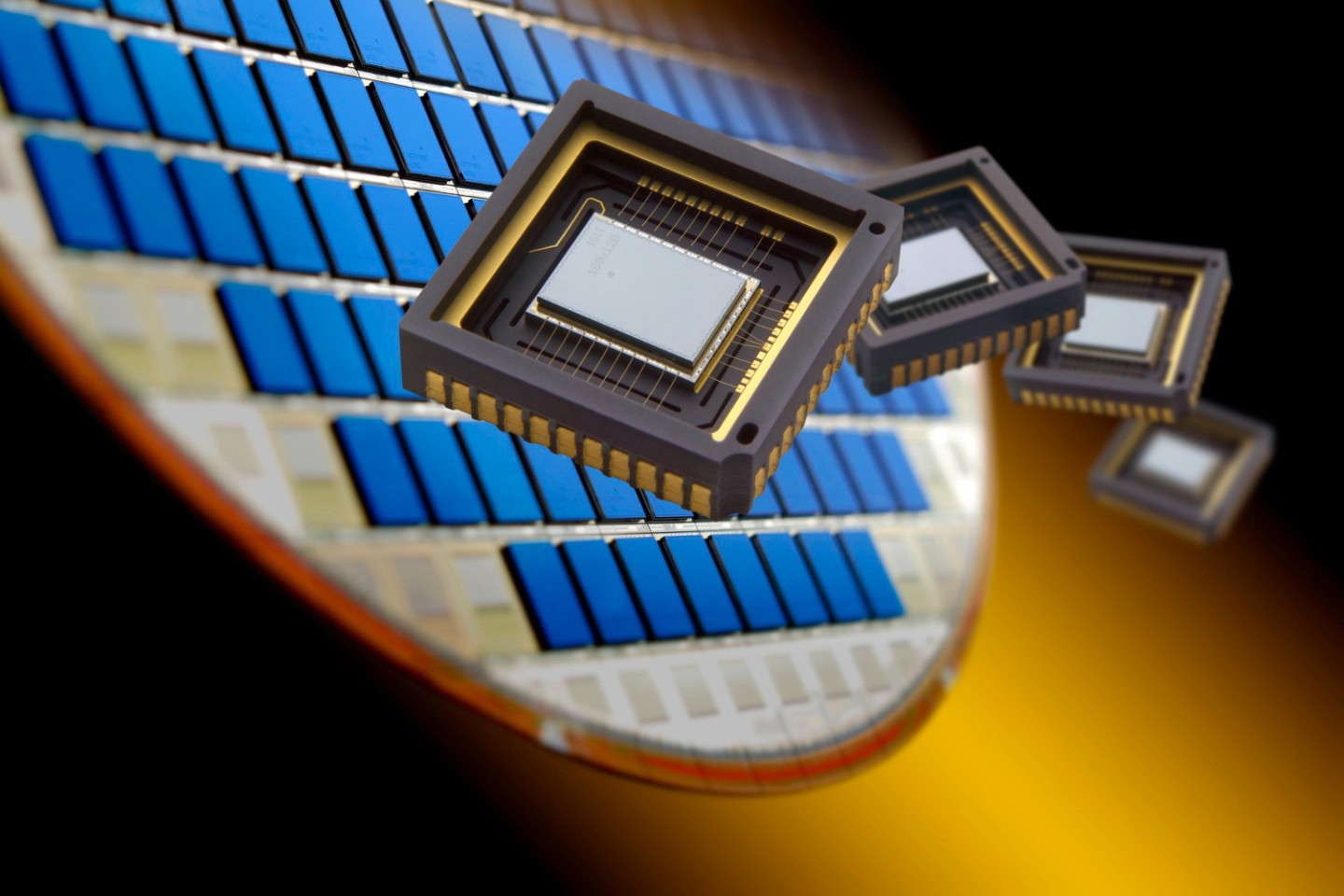
With Europe increasingly dependent on outsourced assembly and testing, advanced packaging and chiplet integration are driving the next generation of smaller, more efficient, and versatile electronic systems, reshaping device manufacturing and functionality.