Simplifying the design process of chiplet-based systems by provision of foundational chiplet building blocks & methods for chiplet selection
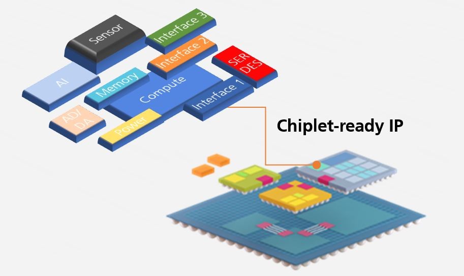
Provision of IPs and chiplets that cover analog, RF, compute & AI, Interfacing, power management, opto, MEMS in (Bi)CMOS and III-V processes
Enablement of System Technology Co-Optimization (STCO) design of chiplet-based systems by provision of models for IPs and chiplets
Validation in demonstrator systems: HPC, Sensing, Photonics, RF
Innovations
Consistent representation by model – IP – chiplet
DfX on IP & chiplet level:
Design for Manufacturing (DfM), Design for Reliability (DfR), Design for Security (DfS), Design for Test (DfT)
Initiation of an ecosystem for chip IP components by establishing systematics and design capabilities: making IPs and dies “chiplet-ready”
Impact
Building links to the European design platform, to make “From Lab to Fab“ in the field of heterogeneous integration easier and more accessible for EU companies to use new technologies and functionalities