Wafer level packaging

Miniaturization meets high performance

© Fraunhofer IZM / Volker Mai
© Fraunhofer IZM
© Fraunhofer IZM
4-layer RDL on Si interposer (Fraunhofer-funded project “STXmod”)

Target:

The demands placed on modern electronic systems are constantly growing: ever smaller designs, increasing performance requirements, lower energy consumption, and high reliability throughout the entire life cycle. Wafer-level packaging (WLP) offers answers to many of these challenges – and Fraunhofer is one of the world's leading institutes for research and development in this field.

Impact:

Fraunhofer sees itself as a link between research and application. In addition to developing innovative processes, the institute supports the industry in different ways:

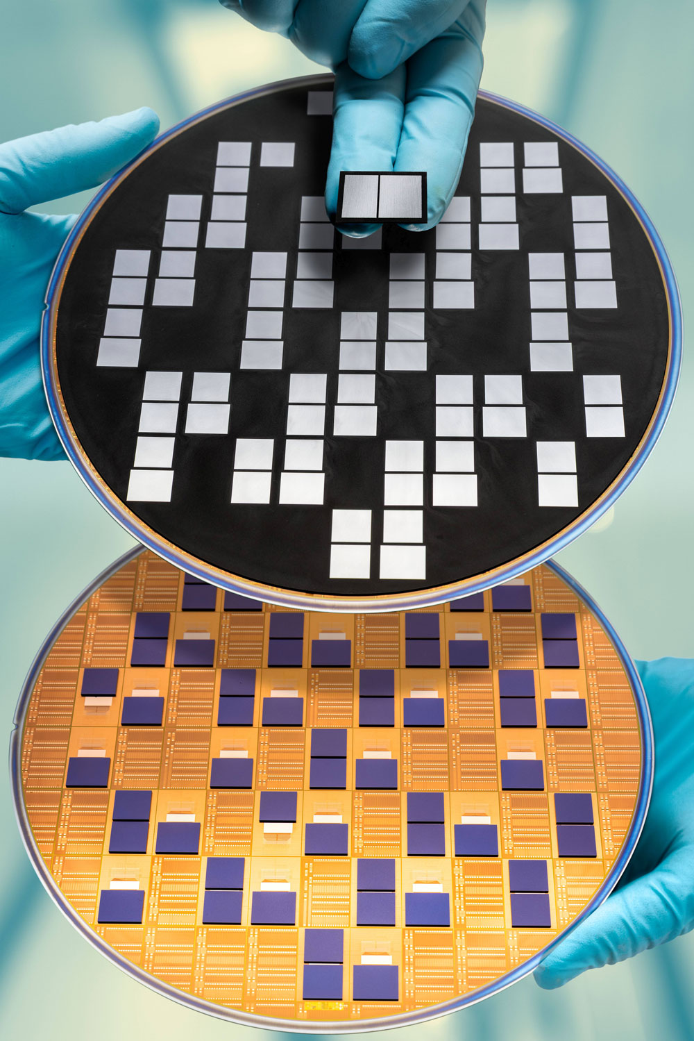
  • Pilot line production and advanced prototyping utilizing in-house clean room
  • Support with design, layout, and simulation
  • Training, technology consulting, and IP transfer


Innovations:

Fan-in and fan-out wafer-level packaging (WLP)

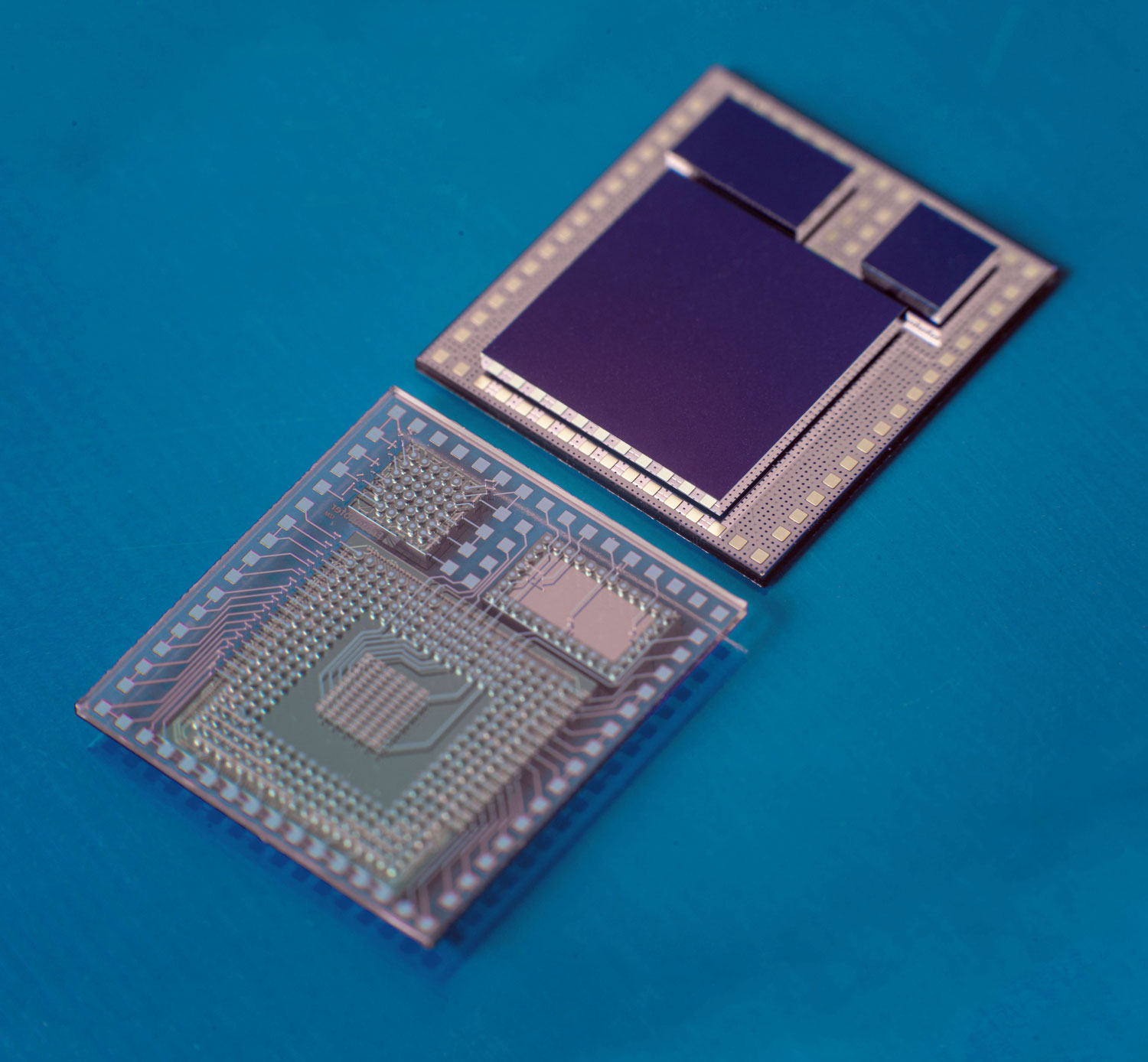
Fan-in WLP is the classic form of WLP, in which the redistribution layer (RDL) is located within the original chip area. This method is particularly suitable for components with a low to medium number of connections – e.g., in mobile devices or sensor applications.

Fan-out WLP (FOWLP), on the other hand, allows the contact areas to be placed outside the original chip area by first embedding the chip in a carrier material and then redistributing it. This allows significantly higher I/O densities and is particularly interesting for complex high-performance applications.

  • Process development for FOWLP, including chip embedding and RDL
  • Multi-die fan-out packaging (e.g., heterogeneous integration of logic + memory)
  • Ultra-thin packages for high-density applications


Redistribution layer (RDL)

The redistribution layer is a core component of every WLP solution. It relocates the electrical contacts from the original pad layout to a new, adapted grid – for example, in preparation for bumping or for connection to other substrates.

  • Development of thin, multilayer RDL structures at wafer-level
  • Use of innovative materials such as thin, low-temperature PI dielectrics
  • Fine-pitch layouts down to <5 µm line/spacing with high manufacturing yield
  • Combination with through-silicon vias (TSVs) for vertical connections
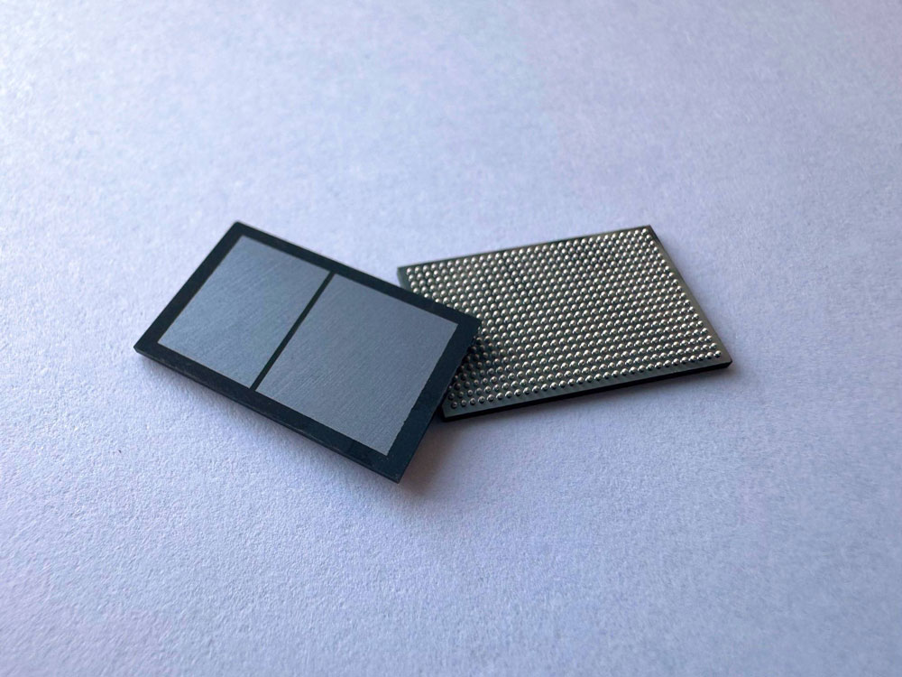
  • Fine-pitch and ultra-fine pitch bump interconnects with a wide variety of bumping metals like Cu/Sn(Ag), Cu/Sn, Ni/Au, Au, AuSn, nano-porous Au (NPG), In, InSn tailored for specific applications
© Fraunhofer IZM
Glass interposer with test chiplets

Interposer technologies (Si, glass and organic) and 2.5D integration

Interposers are intermediate carriers used for signal, mechanical, and thermal connections between chips or between chips and printed circuit boards. Silicon interposers offer high precision and integration density, while organic interposers are more cost-effective and flexible in processing.

  • Design and manufacture of silicon interposers with TSVs, glass interposers with TGVs and SiC interposers with TSiCVs
  • Manufacture of organic interposers for large-scale multi-chip modules 
  • Integration of passive components (e.g. capacitors, resistors) directly into the interposer
  • Integration of bridge elements to realize high-end performance packages
  • Assembly of chiplets and other components (e.g., capacitors, resistors) directly onto the interposer using various assembly techniques (e.g. reflow solder, thermocompression binding transient liquid phase bonding, hybrid bonding)

3D integration & through-silicon vias (TSVs)

Vertical integration via TSVs is a key factor in the realization of true 3D systems — i.e. stacked chips with direct electrical connections through the silicon. This shortens signal paths, improves performance, and reduces space requirements.

  • TSV processing (etching, insulation, metallization) for wafers and dies
  • 3D stacking via thermocompression or hybrid bonding 
  • Heterogeneous integration (e.g. sensor + logic + memory in a stack) 
  • Thermal test chips for thermal dissipation evaluation of packaging

Substrate-Embedded Packaging

Here, active and passive components are embedded directly into carrier materials – such as printed circuit boards, substrates, or mold composites. This results in extremely flat, robust, and reliable modules.

  • Chip-in-polymer and chip-in-board technologies
  • Construction of 3D modules with integrated passive components
  • Realization of extremely flat designs (< 500 µm module height)


Reliability and testing procedures

Modern electronics must function reliably even under extreme conditions – from high temperatures and mechanical stress to moisture and chemical influences. That is why Fraunhofer not only develops packaging technologies, but also comprehensive testing and qualification procedures.

  • Wafer-level reliability testing (including thermal cycles, humidity, shock)
  • Electromigration, thermo-mechanics, and lifetime analyses
  • Development of calibrated FEM models for predictive failure analysis (digital twin)


Multi Project Technologies (MPT)

Multi Project Technologies (MPT) are giving an extended group of customers access to specific standardized process steps that can be therefore made available for the customers own projects. This implies a high Technology Readiness Level of at least TRL ≥ 7. Examples of our MPWs are:

  • SiGe-BiCMOS Technologies and Modules
  • Multi-Project Fan-Out Wafer Level Packaging (MPFOWLP) technologies
  • ASIC Foundry Services

High cost reduction potential

Due to the versatile application possibilites of these technologies, a cost reduction for the end customer is very common, as production start-up costs can be reduced significantly through the use of MPTs.

Further financial advantage through multi-project wafers (MPW)

Multi-project wafers (also multi-purpose wafers) can create a further financial advantage. Usually the costs for lithography mask sets are very high; though they can be shared through MPWs. In this case, the interested customers own design can be placed on the reticle. This leads to a cost reduction of up to 90 % compared to an own development process without a partner.

MPW Runs are especially beneficial in the following scenarios:

• Product Prototyping,

• IP verification, design libraries,

• Device characterization,

• Low volume manufacturing,

• "Proof of concept" for research and development projects,

• Experiments with new circuits/ First Silicon verification.

In addition, this service helps you to get to market faster ("Time to Market").