 APECS – European pilot line for advanced packaging and heterogeneous integration
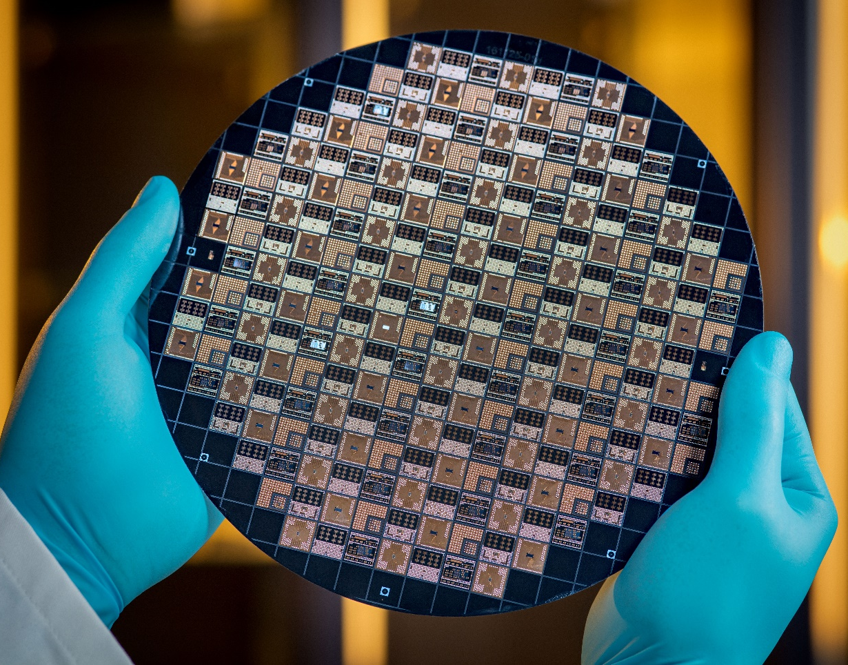
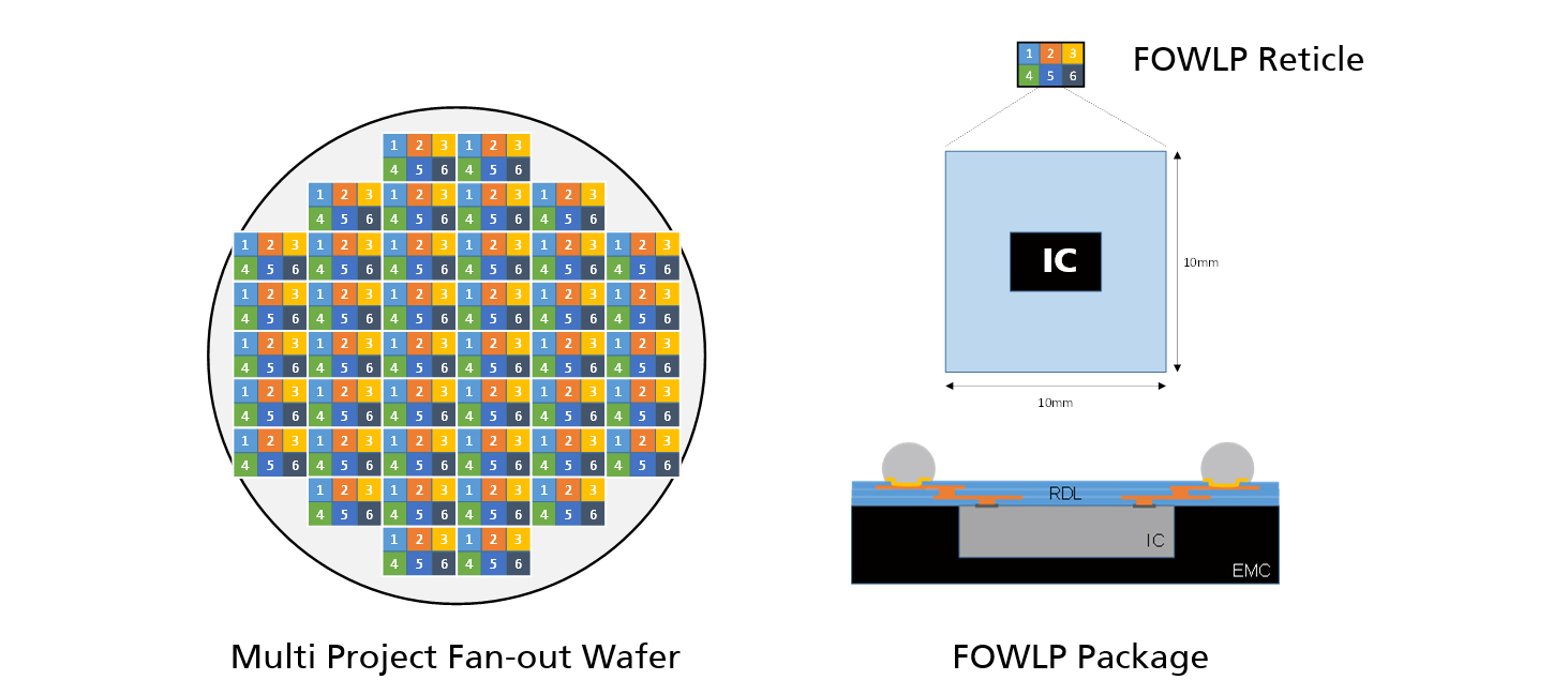
This offering combines two complementary prototyping platforms in APECS into a single System-in-Package (SiP) solution. IHP's SG13G3Cu supplies its fastest silicon-based RF front-end, with SiGe:C HBTs on a low-loss 8-layer copper back-end. Fraunhofer IZM's Multi-Project Fan-Out Wafer Level Packaging (FOWLP) supplies a substrate-less, RF-optimised package in which dies are embedded in mould compound and contacted through a thin-film redistribution layer (RDL). Together, the two technologies close the gap between outstanding transistor performance and the packaging bottleneck that otherwise limits the achievable system bandwidth. As both platforms are organized on a shared-wafer basis, companies, start-ups, universities, and research institutes can access a complete die-to-package prototyping chain at a fraction of the cost of a dedicated wafer run.
© Volker Mai/ Fraunhofer IZM
Multi-project wafer runs
Small volume manufacturing of high-speed BiCMOS dies followed by RF-optimised fan-out packaging
Combined system specifications
Die — SG13G3Cu (IHP)
- SG13G3Cu combines the SG13G3 front-end of IHP with an eight-layer copper back-end from XFAB for highest-performance
- IHP´s SiGe heterojunction bipolar transistors reach transit frequencies of up to 470 GHz and maximum oscillation frequencies of up to 650 GHz
- Die size > 1x1 mm² and < 8x8mm²
Package — FOWLP (IZM)
- Die embedding in epoxy mould compound for a substrate-less and compact system
- RDL-last and face-down die assembly approach with 2 Cu RDL layers
- Package size: 10 × 10 mm²
- Package thickness: 300 μm thick
- Antennas and passive structures can be optionally integrated in the RDL by customer design
- Pin-out via BGA, ball size: 300 µm
Advantages of combining these technology building blocks
The two Multi-Project Wafer Runs at IHP and Fraunhofer IZM are synchronized to manufacture optimized RF-system-in-package solutions in small volumes. This combination shows four key advantages:
High-frequency performance: Short, direct interconnects between the RF chip and the package help reduce parasitic effects that can limit signal quality at high frequencies. The combination supports the transition from high-performance RF ICs to compact system-level prototypes.
Low-loss RF integration: The SiGe:C technology and RF-oriented fan-out package are designed to work together across the signal path. This supports efficient signal transmission between the die, package interconnects and external system interface, with performance optimised through chip-package co-design.
Accessible prototyping: The shared and synchronized Multi-Project Wafer Runs approach gives companies, start-ups, universities and research organisations access to advanced RF system-in-package development without requiring a dedicated manufacturing run. It supports a faster path from chip concept to package prototype.
Low volume prototyping, multi project fan-out-wafer, level packaging
Target applications
The combined APECS offering is intended for small volume mmWave to sub-THz systems in which high-performance front-end electronics and compact, low-parasitic packaging need to be developed together.
Relevant applications include radar applications operating at D-Band and beyond, high-frequency imaging, spectroscopy and industrial sensing. The offering is also relevant for prototyping for example mmWave wireless links, 5G and future mobile networks, high-speed optical transceiver electronics, and wireless sensor networks. Further target areas include medical technology, test and measurement, aerospace and security-related RF systems, where compact heterogeneous integration and early chip-package co-design are important. Final application suitability is assessed individually based on the IC design, package layout and application-specific qualification requirements.
Design flow and access
Die designs are developed using a design flow for analogue, RF and mixed-signal circuits based on IHP´s SG13G3Cu PDK and package development follows Fraunhofer IZM’s FOWLP design rules and layertable. Early chip-package co-design is recommended, for instance RF pad layout, die thickness and package RDL should be aligned from the start to support signal integrity and reliable package integration.
Following design review and acceptance, fabrication is performed through an IHP Multi-Project Wafer Run with tape-in planned in July 2027 and subsequent integration in an IZM Multi-Project FOWLP Run. Final design rules, run scheduling, prices and registration module will be published until February 2027 via an APECS Open Access Call.