Overview
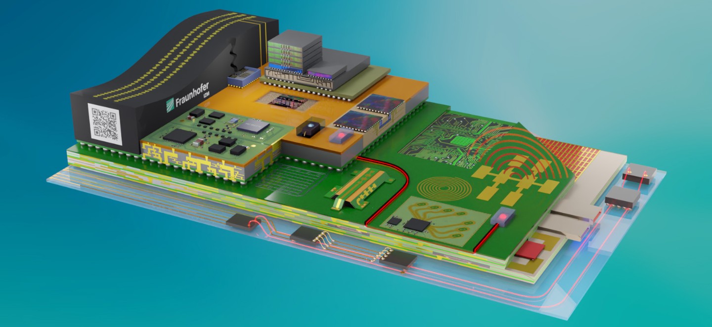
Within APECS, we develop the Chiplet Integration Platform for 2.5D and 3D integration, enabling functional, scalable, and high‑performance chiplet-based systems across RF, photonic, MEMS and heterogeneous applications. We advance functional interposers in silicon, glass, ceramic and organic technologies, targeting ultra‑high-density redistribution layers, TSV/TGV structures, integrated passive devices, and added functionalities such as optical waveguides, thermal management and stress‑control layers. We establish functional integration methods including side‑by‑side and stacked architectures on 200/300 mm wafers and develop advanced packaging approaches such as micro‑transfer printing, volumetric integration and high‑reliability assembly.
We offer advanced interconnection and integration technologies including balling on organic substrates with solder preforms, wafer-level balling with solder preforms, wafer-level bumping, and micromagnets integrated in glass. Our solutions enable highly reliable electrical connections, precise assembly processes, and novel functional integration for next-generation electronic and microsystem applications. By combining scalable manufacturing approaches with innovative material integration, we help partners achieve robust performance, increased design flexibility, and accelerated time-to-market.