Overview
Within APECS, we develop advanced characterization tools and methods for chiplets and QMI systems covering diverse signal types (DC, RF, high-speed digital, mm-wave, and optical), enabling highly accurate and low-noise measurements of heterointegrated devices, sub-THz dielectric material characterization, and the identification of technology weaknesses to validate design and simulation models at chiplet, module, and system levels.
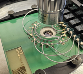
We provide cleanroom-based facilities for wafer- and chip-level testing of optical, RF, and mm-wave signals (up to 80 V and 18 GHz), including dedicated test heads, enabling highly accurate and low-noise evaluation of heterointegrated devices as well as efficient volume-testing methods that deliver statistically relevant feedback for technology development and pilot fabrication.
We offer comprehensive reliability testing and failure analysis capabilities for chiplets and heterointegration (HI), enabling the identification of technology- and application-related defect risks, new failure modes, and degradation mechanisms, while integrating quality and reliability considerations into development to ensure robust design, manufacturing quality, and stable long-term device performance.
We implement architecture-level security measures and security IP blocks from chiplet and heterointegrated devices up to the system level, establish a robust framework to ensure hardware security along the entire manufacturing chain, and characterize and enhance device and system resilience against physical attacks.