Target
- Development and fabrication of multi-layer electronic interconnection architectures based on resin layers which typically include specific filler particles or glass cloths (organic substrates)
- Cover a wide range of applications from ultra dense chip interposers to high power applications using adapted materials and process approaches
- Large area panel level fabrication using advanced printed circuit board process technologies
- Organic substrate processes as basis for heterogeneous integration of single or multiple electronic components into the substrates
- Improvement of electronic functionality and reliability and size reduction of systems or packages at the same time
Innovations
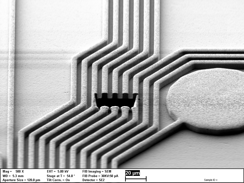
- Fine line processing down to 2 µm line/space copper interconnects in multilayer circuit architectures with ABF/BU dielectric
- Vertical interconnect with diameter down to 10 µm
- Use of glass panels in the core of organic multilayers
- Implementation of specific materials for applications in high frequency, power, and medical electronics respectively
Impact
- Next generation high routing density interposer fabrication
- 6G and beyond miniaturized system
- Power electronic modules with highest efficiency and reduced weight and volume
- Highly versatile set of process technologies for a multitude of applications
 APECS – European pilot line for advanced packaging and heterogeneous integration