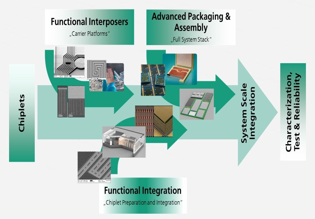
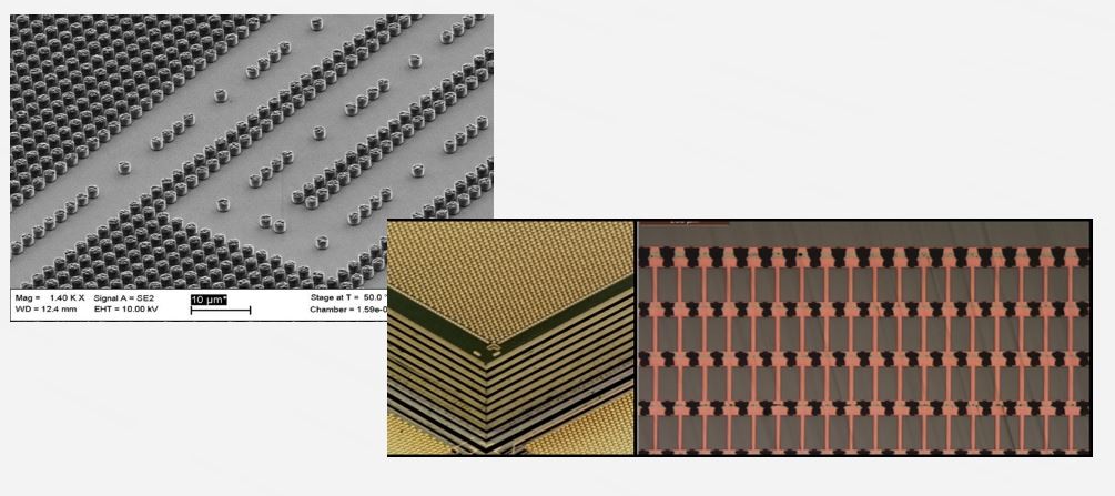
2.5 and 3D stack HD integration of heterogeneous devices for silicon and non-silicon devices with µTSVs in the sub-µm range using microbumps and hybrid bonding innovations
MEMS and Sensor Integration with 3D stacked chiplets up to 300 mm wafers for highly functional modules
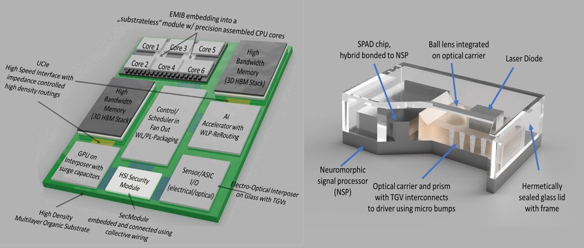
Scale-up of process implementation using embedding technologies into advanced substrates up to 600mm
Module and subsystem integration HPC, NGC, Power-E, Sensors, UWBG & RF/Opto from chiplet to substrate
Scale-up of process implementation for high-end chiplet architectures (3D, 2.5D) up to 600 mm
Open Access for other Pilot Lines, RTO´s and industry to facilitate early adoption of new technologies & fast-track innovations